- 您现在的位置:买卖IC网 > Sheet目录308 > ADUM7241CRZ-RL7 (Analog Devices Inc)ISOLATOR DGTL 1KVRMS 2CH 8SOIC
�� ��
��
��ADuM7240/ADuM7241�
�APPLICATIONS� INFORMATION�
�PRINTED� CIRCUIT� BOARD� LAYOUT�
�The� ADuM7240� /� ADuM7241� digital� isolators� require� no�
�external� interface� circuitry� for� the� logic� interfaces.� Power� supply�
�bypassing� is� strongly� recommended� at� both� input� and� output�
�supply� pins:� V� DD1� and� V� DD2� .� The� capacitor� value� should� be�
�between� 0.01� μF� and� 0.1� μF.� The� total� lead� length� between� both�
�ends� of� the� capacitor� and� the� input� power� supply� pin� should� not�
�exceed� 20� mm.�
�In� applications� involving� high� common-mode� transients,� it� is�
�important� to� minimize� board� coupling� across� the� isolation� barrier.�
�Furthermore,� users� should� design� the� board� layout� so� that� any�
�coupling� that� does� occur� affects� all� pins� on� a� given� component�
�side� equally.� Failure� to� ensure� this� can� cause� voltage� differentials�
�between� pins� exceeding� the� absolute� maximum� ratings� of� the�
�device,� thereby� leading� to� latch-up� or� permanent� damage.�
�With� proper� PCB� design� choices,� the� ADuM7240� /� ADuM7241�
�can� readily� meet� CISPR� 22� Class� A� (and� FCC� Class� A)�
�emissions� standards,� as� well� as� the� more� stringent� CISPR� 22�
�Class� B� (and� FCC� Class� B)� standards� in� an� unshielded�
�environment.� Refer� to� AN-1109� for� PCB-related� EMI� mitigation�
�techniques,� including� board� layout� and� stack-up� issues.�
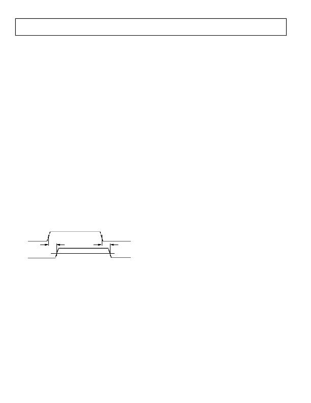
�PROPAGATION� DELAY-RELATED� PARAMETERS�
�Propagation� delay� is� a� parameter� that� describes� the� time� it� takes�
�a� logic� signal� to� propagate� through� a� component.� The� input-to-�
�output� propagation� delay� time� for� a� high-to-low� transition� may�
�differ� from� the� propagation� delay� time� for� a� low-to-high�
�transition.�
�Data� Sheet�
�Channel-to-channel� matching� refers� to� the� maximum� amount�
�that� the� propagation� delay� differs� between� channels� within� a�
�single� ADuM7240� /� ADuM7241� component.�
�Propagation� delay� skew� refers� to� the� maximum� amount� the�
�propagation� delay� differs� between� multiple� ADuM7240� /�
�ADuM7241� components� operating� under� the� same� conditions.�
�DC� CORRECTNESS�
�Positive� and� negative� logic� transitions� at� the� isolator� input�
�cause� narrow� (~1� ns)� pulses� to� be� sent� to� the� decoder� via� the�
�transformer.� The� decoder� is� bistable� and� is,� therefore,� either� set�
�or� reset� by� the� pulses,� indicating� input� logic� transitions.� In� the�
�absence� of� logic� transitions� at� the� input� for� more� than� ~1� μs,� a�
�periodic� set� of� refresh� pulses� indicative� of� the� correct� input� state�
�is� sent� to� ensure� dc� correctness� at� the� output.� If� the� decoder�
�receives� no� internal� pulses� for� more� than� approximately� 5� μs,�
�the� input� side� is� assumed� to� be� unpowered� or� nonfunctional,�
�and� the� isolator� output� is� forced� to� a� default� high� state� by� the�
�watchdog� timer� circuit.�
�MAGNETIC� FIELD� IMMUNITY�
�The� magnetic� field� immunity� of� the� ADuM7240� /� ADuM7241� is�
�determined� by� the� changing� magnetic� field,� which� induces� a�
�voltage� in� the� transformer’s� receiving� coil� large� enough� to� either�
�falsely� set� or� reset� the� decoder.� The� following� analysis� defines�
�the� conditions� under� which� this� can� occur.� The� 3� V� operating�
�condition� of� the� ADuM7240� /� ADuM7241� is� examined� because�
�it� represents� the� most� susceptible� mode� of� operation.�
�The� pulses� at� the� transformer� output� have� an� amplitude� greater�
�INPUT� (V� Ix� )�
�OUTPUT� (V� Ox� )�
�t� PLH�
�t� PHL�
�50%�
�50%�
�than� 1.0� V.� The� decoder� has� a� sensing� threshold� at� about� 0.5� V,� thus�
�establishing� a� 0.5� V� margin� in� which� induced� voltages� can� be�
�tolerated.� The� voltage� induced� across� the� receiving� coil� is� given� by�
�V� =� (� ?dβ/dt� )� ∑� π� r� n� 2� ;� n� =� 1,� 2,� …� ,� N�
�Figure� 13.� Propagation� Delay� Parameters�
�Pulse� width� distortion� is� the� maximum� difference� between�
�these� two� propagation� delay� values� and� is� an� indication� of� how�
�accurately� the� timing� of� the� input� signal� is� preserved.�
�where:�
�β� is� the� magnetic� flux� density� (gauss).�
�r� n� is� the� radius� of� the� n� th� turn� in� the� receiving� coil� (cm).�
�N� is� the� number� of� turns� in� the� receiving� coil.�
�Given� the� geometry� of� the� receiving� coil� in� the� ADuM7240� /�
�ADuM7241� and� an� imposed� requirement� that� the� induced�
�voltage� be,� at� most,� 50%� of� the� 0.5� V� margin� at� the� decoder,� a�
�maximum� allowable� magnetic� field� at� a� given� frequency� can� be�
�calculated.� The� result� is� shown� in� Figure� 14.�
�Rev.� A� |� Page� 12� of� 16�
�发布紧急采购,3分钟左右您将得到回复。
相关PDF资料
ADUM7440CRQZ-RL7
IC DIGITAL ISOLATOR 4CH 16QSOP
ADUM7510BRQZ
IC DGTL ISOLATOR 5CH 16QSOP
ADZS-21364-EZLITE
KIT EVAL EZ LITE ADDS-21364
ADZS-21371-EZLITE
KIT EVAL EZLITE ADZS-21371
ADZS-21469-EZLITE
KIT EVAL EZ LITE ADSP-21469
ADZS-21479-EZLITE
KIT EVAL EZ BOARD ADSP-2147X
ADZS-21489-EZLITE
KIT EVAL EZ BOARD ADSP-2148X
ADZS-218X-ICE-2.5V
EMULATOR SRL FOR ADDS-218X-ICE
相关代理商/技术参数
ADUM7410BRQZ
制造商:Analog Devices 功能描述:
ADUM7410BRQZ-RL7
制造商:Analog Devices 功能描述:
ADUM7410BRWZ
制造商:Analog Devices 功能描述:
ADUM7410BRWZ-RL
制造商:Analog Devices 功能描述:
ADUM7440ARQZ
功能描述:IC ISOLATOR DGTL QUAD 16QSOP RoHS:是 类别:隔离器 >> 数字隔离器 系列:iCoupler® 标准包装:66 系列:iCoupler® 输入 - 1 侧/2 侧:2/2 通道数:4 电源电压:3.3V,5V 电压 - 隔离:2500Vrms 数据速率:25Mbps 传输延迟:60ns 输出类型:逻辑 封装/外壳:20-SSOP(0.209",5.30mm 宽) 供应商设备封装:20-SSOP 包装:管件 工作温度:-40°C ~ 105°C
ADUM7440ARQZ
制造商:Analog Devices 功能描述:IC DIGITAL ISOLATOR 50NS QSOP-16 制造商:Analog Devices 功能描述:IC, DIGITAL ISOLATOR, 50NS, QSOP-16
ADUM7440ARQZ-RL7
功能描述:IC DIGITAL ISOLATOR 4CH 16QSOP RoHS:是 类别:隔离器 >> 数字隔离器 系列:iCoupler® 产品培训模块:IsoLoop® Isolator 标准包装:50 系列:IsoLoop® 输入 - 1 侧/2 侧:5/0 通道数:5 电源电压:3 V ~ 5.5 V 电压 - 隔离:2500Vrms 数据速率:110Mbps 传输延迟:12ns 输出类型:CMOS 封装/外壳:16-SOIC(0.154",3.90mm 宽) 供应商设备封装:16-SOIC N 包装:管件 工作温度:-40°C ~ 85°C 其它名称:390-1053-5
ADUM7440BRQZ
制造商:Analog Devices 功能描述: